x86 gets the boot as Google pairs up its TPUs with some Arm-based Axion cores
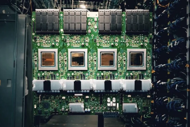
Google unveiled two new in-house AI accelerators at its annual Cloud Next conference in Las Vegas on Wednesday: one designed to speed up training and another aimed at driving down model serving costs.
The Chocolate Factory boasts its eighth-gen tensor processing units are as much as 2.8x faster in training and deliver 80 percent higher performance per dollar for LLM inference compared with last year's Ironwood TPUs.
To achieve this, Google has dual-tracked its accelerator development, building the TPU 8t for training and TPU 8i for inference.
While these chips are built on similar foundations, each is specifically aimed at eliminating bottlenecks in its respective workload.
Google isn't the first to go down this road.
Early in its AI chip development, Amazon Web Services recognized the need for inference- and training-optimized accelerators.
Nvidia has also dabbled with this kind of specialization, though not to the same extent.
The GPU slinger's Blackwell Ultra generation was optimized specifically for AI inference, trading high-precision grunt for a 50 percent jump in memory and FP4 compute over its Blackwell sibling.
Google's approach to specialization goes much deeper than the TPUs themselves.
The search and advertising giant has developed new clusters with distinct network topologies to minimize scaling losses across both inference and training.
Modern AI workloads rarely run on a single accelerator these days, so the ability to efficiently scale those workloads across multiple chips is often more important than how fast each one is.
Like its past accelerators, Google's TPU 8t is designed for training at a massive scale.
The company may not draw the same hype as OpenAI or Anthropic, but Google remains a prolific model builder.
Under the hood, Google has tweaked the mix of vector, matrix multiplication, and SparseCore embedding accelerators introduced with its Ironwood chips to maximize effective floating point throughput.
Each accelerator features 216 GB of high-bandwidth memory (HBM) good for 6.5 TB/s of bandwidth, 128 MB of on-chip SRAM, up to 12.6 petaFLOPS of 4-bit floating point compute, and up to 19.2 Tbps of chip-to-chip bandwidth.
Compared to Nvidia's Rubin GPUs , which Google also announced plans to deploy across its cloud infrastructure, the new TPU might look a little tame.
Rubin boasts up to 35 petaFLOPS of FP4 training performance and 288 GB of HBM4 good for 22 TB/s of bandwidth.
So individually, Nvidia's GPUs are faster, but it doesn't really matter: When training a new frontier model, you're not using one GPU, you're using thousands.
And when it comes to scale, Google has the advantage.
Nvidia's latest GPUs support up to 576 accelerators in a single NVLink domain before having to scale out over Ethernet or InfiniBand.
The TPU 8t, on the other hand, uses optical-circuit switches, an opto-mechanic switching technology that works more like a telephone switchboard than a packet switch, to connect up to 9,600 accelerators in a single unified pod.
Multiple pods are then stitched together using its new Virgo Network to support even larger compute domains.
Rather than just building a bigger chip-to-chip mesh, Google appears to be using packet switches with extremely high port densities.
As we understand it, these are arranged in a flat-ish two-tier all-to-all topology capable of connecting up to 134,000 TPUs per datacenter and up to a million TPUs when connecting multiple sites.
Or so Google claims.
Alongside the new network fabric, Google has also developed a Managed Lustre storage system capable of delivering 10 TB/s of aggregate data directly into its accelerators' memory.
According to Google, these technologies, combined with improved reliability, availability, and serviceability (RAS) capabilities will enable its training-optimized TPUs to operate at a "goodput" of 97 percent.
In this case, goodput means the amount of time the TPUs actually spend training.
"Every hardware failure, network stall, or checkpoint restart is time the cluster is not training, and at frontier training scale, every percentage point can translate into days of active training time," the company explained in a blog post.
TPU 8i: An inference inflection
Inference is an auto-regressive workload, which means that for each token generated, the entire model's active weights need to be streamed through memory.
While compute is still important, the main bottleneck tends to be memory bandwidth.
For its inference-focused TPU 8i, Google is trading some FLOPS for a much larger SRAM cache and faster, higher-capacity memory pool.
The chip is roughly comparable to Nvidia's Blackwell accelerators on paper.
The TPU 8i features 10.1 petaFLOPS of FP4 compute fed by 384 MB of on-chip SRAM, and 288 GB of HBM good for 8.6 TB/s of bandwidth.
Interconnect bandwidth, meanwhile, is unchanged from its training-focused sibling.
According to Google, all that SRAM helps the TPU 8i keep more of the key-value cache (model's short term memory) resident on chip and reduce the amount of time the cores are left waiting for data.
TPU 8i also ditches Google's SparseCores in favor of a collective acceleration engine (CAE).
As the name suggests, the accelerator block speeds up inference by offloading collective communications, like all-reduce or all-gather, shortening synchronization stalls that would otherwise leave the chip's tensor cores sitting idle.
In fact, Google's focus with TPU 8i appears to be killing as much latency across the inference stack as it can.
Collective communications have become quite problematic as mixture-of-experts (MoE) architectures have become more common.
These models are made up of multiple submodels, appropriately called experts, a subset of which are activated for each token generated.
The benefit is models can grow larger without necessarily requiring additional memory bandwidth to maintain the same level of performance.
The downside is that chip-to-chip communication is less predictable, as generating one token might use a different set of experts from the next, and those experts might be on different accelerators.
Google says its CAE reduces collective communication latencies five-fold, which translates into better economics by allowing them to pack more users onto the same hardware.
Alongside its inference-optimized chips, Google has also developed a topology called Boardfly.
The network arrangement is somewhat reminiscent of the Dragonfly topologies commonly employed in HPC clusters, and allows 1,152 chips (1,024 active at any given moment) to be connected using optical circuit switches.
The key advantage of Boardfly is it cuts the maximum chip-to-chip latency from 16 hops in a 3D torus to just seven hops, further reducing the chip-to-chip latency when running a MoE or reasoning models.
Google isn't the only one that's changed the way it builds its inference clusters to better accommodate emerging architectures.
In December, AWS ditched 3D toruses for inference for similar reasons, but opted instead for a more conventional packet switched fabric.
Both TPU 8 accelerators will be generally available later this year in Google Cloud Platform as instances, or as part of the cloud provider's full-stack AI Hypercomputer platform, which bundles up all the networking, storage, compute, and software required to deploy or train LLMs at scale.
®
Related Stories


Source: This article was originally published by The Register
Read Full Original Article →
Comments (0)
No comments yet. Be the first to comment!
Leave a Comment